
How to Clean PCB Pads After Removing Components
After an electronic component is removed from a circuit board, solder usually remains on the PCB pads. The surface may also contain flux residue, uneven solder, oxidation or small solder bridges.
Before installing a replacement component, these pads should be cleaned and prepared properly. Smooth, intact PCB pads make component alignment easier and help new solder joints form more consistently.
This guide explains how to clean PCB pads after component removal using SATZOZZ Desoldering Wick, SATZOZZ NC559 No-Clean Soldering Flux and controlled soldering techniques.
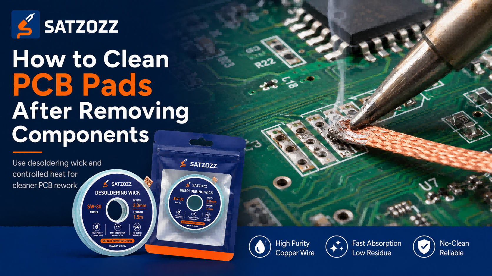
Desoldering wick, no-clean flux and controlled heat can help remove excess solder and prepare PCB pads for component replacement.
Quick answer: Apply a small amount of flux to the remaining solder, place desoldering wick over the PCB pad, heat the braid briefly with a soldering iron and allow it to absorb the molten solder. Lift the iron and wick together, clean the residue if necessary and inspect the pad before installing the new component.
Safety reminder: Disconnect all power sources and batteries before beginning repair work. Use appropriate ESD precautions and avoid prolonged heat on delicate pads.
People Also Ask About Cleaning PCB Pads
How do you remove old solder from PCB pads?
Apply flux to the old solder, place desoldering wick over the pad and heat the wick with a soldering iron. The molten solder moves into the copper braid, leaving the pad flatter and cleaner.
Should PCB pads be completely free of solder?
The pads do not always need to be completely bare. They should be flat, clean and free from excessive solder or bridges so the replacement component can be aligned and soldered correctly.
Can desoldering wick damage PCB pads?
It can if too much heat, pressure or dragging force is used. Apply controlled heat, avoid scraping the board and lift the wick while the solder is still molten.
Do you need flux when using desoldering wick?
Flux is strongly recommended. It helps the remaining solder reflow and improves the transfer of molten solder into the copper braid.
How do you know if a PCB pad is damaged?
A damaged pad may appear lifted, detached, torn, discolored or missing. The copper pad may also move when touched gently with precision tweezers.
Why PCB Pads Need Cleaning After Component Removal
When a component is removed, the original solder rarely disappears completely. Uneven solder deposits can prevent the replacement part from sitting flat on the board.
Cleaning the pads helps technicians:
- Remove excess solder from component footprints
- Identify lifted, missing or damaged pads
- Improve component alignment
- Reduce the risk of new solder bridges
- Prepare a smoother surface for fresh solder
- Inspect the board before continuing the repair
Tools Needed for PCB Pad Cleaning
Desoldering Wick
Desoldering wick absorbs molten solder from PCB pads. Different wick widths are suitable for different component footprints and repair areas.
No-Clean Soldering Flux
Flux helps old solder melt and flow into the desoldering braid more efficiently. Apply only enough to cover the repair area.
Temperature-Controlled Soldering Iron
A temperature-controlled soldering iron provides predictable heat and reduces the risk of overheating delicate PCB pads.
Precision Tweezers
Precision tweezers help remove loose solder fragments, inspect pad stability and position replacement components.
Magnification
A microscope or magnifying tool makes it easier to identify bridges, pad damage and remaining solder around small footprints.
Cleaning Materials
Use suitable electronics cleaning materials, lint-free swabs or brushes when residue needs to be removed before inspection.
How to Clean PCB Pads Step by Step
Step 1: Disconnect Power and Secure the Board
Remove batteries, power supplies and connected cables. Place the circuit board on a stable ESD-safe work surface so it cannot move during cleaning.
Step 2: Inspect the Component Footprint
Use magnification to inspect the pads before applying heat. Look for solder bridges, lifted pads, broken traces, loose fragments or excessive solder deposits.
Step 3: Apply a Small Amount of Flux
Apply flux directly to the remaining solder. A controlled amount is usually sufficient. Too much flux can make the repair area difficult to inspect.
Step 4: Select the Correct Wick Width
Choose a desoldering wick approximately suited to the pad area. Narrow braid is useful for small pads and fine-pitch footprints, while wider braid is more efficient on larger pads.
Step 5: Place the Wick on the Solder
Position a clean section of wick over the solder deposit. Keep the braid flat against the pad without pressing heavily.
Step 6: Apply Controlled Heat
Place the soldering iron tip on top of the wick. As the solder melts, it should move into the copper braid. Remove the heat as soon as the solder has been absorbed.
Step 7: Lift the Iron and Wick Together
Lift the soldering iron and wick together while the solder is still molten. Do not allow the braid to cool and stick to the pad before lifting it.
Step 8: Cut Off the Used Wick
Cut away the solder-filled section. Continue with fresh braid if more solder needs to be removed.
Step 9: Clean and Inspect the Pads
Remove residue if required and inspect the footprint again. The pads should look flat, separated and securely attached to the PCB.
Choosing the Right Desoldering Wick Width
| Model | Width | Recommended Pad-Cleaning Use |
|---|---|---|
| SW-10 | 1.0mm | Ultra-fine pads, small SMD footprints and delicate motherboard repair |
| SW-15 | 1.5mm | Fine-pitch components, small IC pads and phone motherboard work |
| SW-20 | 2.0mm | General PCB pad cleaning and common electronics repair |
| SW-25 | 2.5mm | Medium component footprints and wider solder areas |
| SW-30 | 3.0mm | Larger pads, connectors and higher solder-volume areas |
View all available widths on the SATZOZZ Desoldering Wick product page.
How Much Solder Should Remain on the Pads?
The goal is not always to expose completely bare copper. Removing too much solder can increase heat exposure without providing additional benefit.
Well-prepared pads should generally be:
- Flat enough for the component to sit correctly
- Free from unintended connections between adjacent pads
- Securely attached to the PCB substrate
- Clean enough for visual inspection
- Ready for controlled application of fresh solder
How to Check for Lifted or Damaged Pads
After the solder is removed, inspect every pad carefully. Pad damage is more likely when excessive heat or mechanical force was used during component removal.
Warning signs include:
- A pad rising above the board surface
- A copper pad moving when touched gently
- Missing sections of copper
- Broken traces leading away from the footprint
- Darkening or delamination around the repair area
Use SATZOZZ S-05U Ultra-Fine Precision Tweezers carefully when checking loose fragments or pad stability. Do not pull or scrape the pad.
Common PCB Pad-Cleaning Mistakes
1. Applying Too Much Pressure
Desoldering wick works through heat and capillary action. Heavy pressure does not improve absorption and may damage pads or solder mask.
2. Dragging the Wick Across the Board
Avoid pulling hot braid across the PCB. Place it on the solder, allow it to absorb and lift it vertically with the iron.
3. Heating the Pad for Too Long
Prolonged heating can weaken the adhesive holding the copper pad to the circuit board. Work in short, controlled intervals.
4. Using Solder-Filled Wick
Once a section of wick is filled with solder, its absorption performance decreases. Cut off the used section before continuing.
5. Using Wick That Is Too Wide
Oversized braid can transfer unnecessary heat to nearby components and pads. Match the wick width to the footprint.
6. Installing the New Component Before Inspection
Always inspect pad condition and alignment before applying fresh solder or positioning the replacement component.
Recommended SATZOZZ Tools for PCB Pad Cleaning
- SATZOZZ Desoldering Wick — five widths from 1.0mm to 3.0mm for solder removal and PCB pad cleaning.
- SATZOZZ NC559 No-Clean Soldering Flux Kit — supports solder flow during rework and pad preparation.
- SATZOZZ S-05U Ultra-Fine Precision Tweezers — for small component handling, inspection and precision repair work.
Need Tools for PCB Pad Cleaning?
Explore SATZOZZ desoldering wick, NC559 no-clean flux and ultra-fine precision tweezers for PCB repair, component replacement and electronics rework.
View SATZOZZ Repair Tools →FAQ
What is the best way to remove solder from PCB pads?
Apply flux, place desoldering wick over the solder and heat the braid briefly with a temperature-controlled soldering iron. Allow the wick to absorb the molten solder before lifting it.
Should I add flux before using desoldering wick?
Yes. Flux improves solder flow and helps old solder transfer into the copper braid more efficiently.
Why does desoldering wick stick to PCB pads?
Wick can stick when the solder cools before the braid is lifted. Lift the iron and wick together while the solder remains molten.
Can I reuse the same piece of desoldering wick?
Use a fresh section after the braid becomes filled with solder. Used wick absorbs less efficiently and can increase heating time.
How can I avoid lifting PCB pads?
Use controlled temperature, short heating intervals, minimal pressure and the correct wick width. Never scrape or pull the braid across the pads.
Conclusion
Cleaning PCB pads after component removal is an important part of electronics rework. The objective is to remove excessive solder, inspect the pad condition and prepare a flat, stable footprint for the replacement component.
Use a small amount of flux, choose the correct desoldering wick width and apply controlled heat. Avoid heavy pressure, prolonged heating and dragging the braid across the board.
For everyday PCB pad cleaning and solder removal, SATZOZZ Desoldering Wick provides multiple width options for fine, general and larger repair areas.